Circuit Design ep.2 - Creating a PCB in KiCad
Комментарии:

@bennetting1609 - 07.01.2023 23:23
The GOAT 🐐
Ответить
@mspeir - 13.06.2023 18:28
Press 'V' while routing to place a via on the net. Press 'U' after selecting a segment of a trace to select all segments of the trace.
Ответить
@marsrocket - 31.07.2024 06:43
Great video. In some case I would have rotated the dip 180 degrees to make left near left.
Ответить
@richardmills5450 - 13.10.2024 14:58
You make fabulous videos. I guess you need a lot of practice to get this correct. Cheers
Ответить
@larrybud - 04.12.2024 20:22
"mils" and "thou" are also used most often in machining.
Ответить
@KennethiSlite - 03.01.2025 02:12
Very good work!!
Ответить
@electrarc240 - 09.01.2023 19:20
Corrections:
Copper fills - It is usually better to put the GND fill on the rear and Vdd on the front, as the majority of traces will be on the front slicing up that fill, but connections to GND are more common so that is the more important plane.
Circuit Design ep.2 - Creating a PCB in KiCad
ElectrArc240
We Came for Lunch...& Left With Plants 🪴 || Visit Our Garden
Visit Our Garden
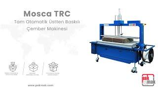
Mosca TRC Tam Otomatik Üstten Baskılı Çember Makinesi
Pakmak Ambalaj
Computer for Banking | Delhi Police | HSSC | Railway | Nagendra Sir | BSC Live | BSC Academy
Tyrasons Publications |Think different keep ahead
SH FIGUARTS DODORIA FIGURE REVIEW
KENNYBOY'S TOYS


